Blog

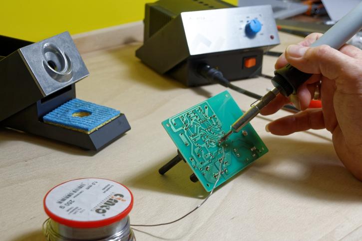
The printed circuit board or PCB is a key concept in the study and manufacturing of the electronics that make our lives more efficient every day. Printed circuit boards were preceded by the laborious process of point to point writing. The creation of this device means that we no longer have to worry about frequent failures at wire junctions and short circuits. To ensure their effectiveness, printed circuit board testing occurs – test points are identified and results are tracked. Often test points will turn green or red to indicate a pass or fail.
Due in part to the rise of the PCB in consumer goods, the double printed circuit board emerged. Compared to the conventional assembly of the single sided PCB, the double sided option is more technical and complex. It involves a number of structured process handling techniques. Read on to learn more about the basics of the design and manufacturing process.
1. Assembly of the Photo Works
The process starts with the creation of the plots for the various components to be mounted. Photo works creation is followed by the creation of corresponding proto plots. The schematic processes are simply translated to the board from the perceived initial process. For the best results, Gerber data is imprinted on the board. Gerber is a file format used to communicate design information to manufacturing for types of printed circuit boards, and is the standard in the electronics industry Repeated testing of the schematic process and comparison with the initial schematic design is continuously done. Printed circuit board testing should be thoroughly done at the end of this phase, if the components are immediately attached on the board.
2. Preparation of the Board
Copper clad panels are best in crafting double sided boards. Once the right board has been identified, partial holes are drilled for the entry material and on the backup boards before trimming them to shape and size. Conventionally a 1.6mm think panel with an 18-micron copper cladding is recommended.
3. Drilling and Pinning
The prospective position for attaching the components is drilled with the appropriate sized tooling equipment. Once complete, the PCB pool panel is pinned on the CNC machine for completion of the pinning process.
4. Finishing up
The PCB production process involves greasing of the board to ease its use under pressure. Upon completion, the board should then be cleaned by brushing off the grease. To ensure optimal results, the components being mounted should undergo rigorous printed circuit board testing to ensure high quality performance. The results of this testing determine the board’s efficiency.
To find out more about PCB assembly and testing, visit our Services page. We produce high-caliber printed circuit boards and provide a prototype quantity upon request!


